CAPABILITIES
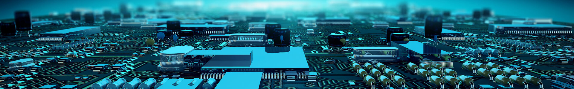
One type of board that is frequently used in the engineering field is the high frequency PCB. These PCBs are well-known for having a variety of attributes. PCBs are essential to the manufacturing of all electronics.
It is important to use high frequency printed circuit boards. A variety of electronics have been produced using this circuit board. We'll be talking about crucial information regarding this PCB that you should be aware of in this post.
What is a High Frequency PCB?
PCBs with high frequencies transfer electromagnetic waves with low loss. Applications requiring the transfer of signals between objects frequently use this kind of PCB. Certain materials must be used during the fabrication of a high frequency printed circuit board.
Signal flow rates are faster on this board. It operates in the vicinity of 100 GHZ. Low levels of thermal expansion, lower DF, and lower DK are provided by high frequency boards. HDI technology frequently uses these circuit boards.
Properties of High Frequency PCB

Wide range of properties are offered by high frequency PCB. You can better understand these PCBs by being aware of these properties. Because of the characteristics these printed circuit boards provide, they are also known as high frequency boards. Let's examine these PCBs' characteristics.
Dissipation factor: The dissipation factor of frequency PCBs is low, ranging from 0.0019 to 0.025. This number aids in preventing any disruptions to the signal transmission rate. Better signal transmission is also made possible by a low dissipation factor. Reducing the dissipation factor can aid in reducing the loss of signal.
Low and stable dielectric constant: A high frequency printed circuit board has a lower and more stable dielectric constant. This contributes to frequency transmission assurance. Less signal delay is also ensured by doing this. Higher frequency transmission rates are correlated with lower dielectric constants.
Chemical resistance: PCBs with a high frequency can tolerate chemicals. If exposed to a chemical attack, these boards can withstand it. These circuit boards are less likely to corrode as a result of this characteristic.
Low rate of water absorption: have a low moisture absorption rate. It is resistant to moisture absorption and can therefore be used in humid environments.
Low dimensional stability: Low dimensional stability is a feature of frequency PCB. No matter what temperature these PCBs are exposed to, they keep their size. Their size doesn't change when they're heated up.
Guidelines for Designing High Frequency PCB
PCB designers need to take some steps when designing high frequency PCB material. Below are steps that need to be taken;
Arrange your design.
It is essential that you have a design in mind before you start designing the PCB. By taking this action, you will be able to avoid any potential problems with your design. Creating a checklist is a crucial step in this process.
Find the frequency of the PCB signal.
Make sure you ascertain the integrated circuits' power and voltage requirements. Make a decision regarding any power plane divisions. It's also necessary to confirm that various signals can be supported. The manufacturer contributes to ensuring that the minimal tolerance requirements are met. Having a strategy in place to lower the noise level on your high-frequency signals is crucial.
Create a board stacking plan for manufacturing.
It is crucial to document the requirements for the stack up layer as soon as you decide how to design the printed circuit board. To find out the precise material for your PCBs, you can ask the manufacturer for assistance. It's critical that you comprehend the particular limitations and components of your printed circuit board.
Make a floor plan.
Your PCB needs to be divided into sections for floor planning. You must decide whether to incorporate your subcircuits into a larger design. When there are analog and digital components that must be carefully isolated to minimize interference, this is crucial.
Ascertain the ground planes and power
This is a crucial phase to take. You must review your HDI PCB design after defining the PCB layout. Understanding the ground plane is essential. It might not be necessary to use a routed signal to split the ground plane.
The ground plane splitting suggests that the void needs to be rotated. This could have an impact on EMI and signal timings. The ground plane must be divided. Ensure that the signal trace has a resistor in it. This will facilitate a gap in the signal, improving the return path.
Diminish the extent of land patterns
Little pad is a common feature on high frequency PCBs. Comparing their pads to other PCBs, they are smaller. Cutting down on PCB space contributes to the PCB's useful life. Additionally, you can keep the pad size the same as the component pin size.
Cutting back on space has many advantages. By doing this, the mechanical strength will rise and the parasitic capacitance will be reduced. More room for different pairs will be available if the area is reduced.
Send the frequency signals via a route.
You must route your frequency signals if you wish to take advantage of this board's additional shielding benefits. High radiation is produced by high-frequency signals. This may result in interference between two different signals. You can help avoid this by routing the frequency signals.
Create a good current return path: Each signal on a high frequency printed circuit board needs a path. The path takes you from the source to the sink at the end of the route. Little impediment is necessary for the path. This plays a crucial role in the creation of radio frequency substrates.
Sometimes using a via is necessary to ensure that the path stays clear. If you don't do this, the currents on your ground plane will probably spread over divisions.
Reduce trace coupling by using the 3W rule: Line coupling can pose a significant threat to signal integrity during transmission. This can be decreased with the aid of the 3W rule. By following this rule, the coupling effect will be minimized as there will be an increase in the distance between the traces.
Reduce plane coupling by using the 20H rule: Your PCB design may be at risk if there is coupling between the ground and power planes. The 20H rule states that you must ensure that the space between the neighboring ground and power planes is significantly thicker than the power plane.
Fabrication Process for High Frequency PCBs

High-frequency circuit boards are made using a simple fabrication process. Making a PCB is quite simple if you can comprehend a few factors.
Create a PCB design as your initial step. The location of the PCB blueprint must be planned at this point. Designer software such as Extended Gerber can assist you with your design.
Print PCB design: In this section, your PCB design is printed. Printing is done using a plotter printer. A PCB film is produced by this printer. There are two different kinds of ink used in this movie: clear and black. The PCB's non-conductive regions are visible thanks to the clear ink. Black ink is used by the board's circuit and copper.
Print copper for the inner layers: This is the point at which PCB production begins. The copper will be pre-bonded on the precise laminate that acts as the PCB structure after the PCB has been printed on it. Engraving the copper can reveal the original PCB blueprint.
Layer alignment: The layers must be in line when manufacturing high frequency printed circuit boards. Both the inner and outer PCB layers can be arranged using the holes.
Lamination of PCB layers: In this case, the PCB and the lay-up procedures are laminated. After the outer and inner layers are ready, assemble them. You can join the layers with the aid of a metal clamp.Print copper for the inner layers: This is the point at which PCB production begins. The copper will be pre-bonded on the precise laminate that acts as the PCB structure after the PCB has been printed on it. Engraving the copper can reveal the original PCB blueprint.
Layer alignment: The layers must be in line when manufacturing high frequency printed circuit boards. Both the inner and outer PCB layers can be arranged using the holes.
Lamination of PCB layers: In this case, the PCB and the lay-up procedures are laminated. After the outer and inner layers are ready, assemble them. You can join the layers with the aid of a metal clamp.
Drilling: You can identify the drilling spots with the aid of an X-ray machine. The circuit board can then be secured with the help of drill holes. When the drilling is finished, the excess copper can be filed off.
Plating of PCB: Chemicals are required for PCB plating. You can sandwich the layers together with the aid of these chemicals. Make sure the board is clean before applying any chemicals.
Solder masking: In this case, cleaning the panel is required prior to solder mask application. There will be applications of solder film and epoxy ink.Silk screening and finishing: The PCB will either have HASL, silver, or gold plating applied to it. The copper and the pad will be shielded as a result. After plating, the PCB is silk-screened.
Testing: You must test your circuit board to make sure it operates properly. Among these tests are the isolation and circuit continuity tests.
Cutting: After testing your PCB, you can cut a few pieces off of the PCB panel. A CNC machine or a V-a groove can be used to cut PCBs.
High Frequency PCB Applications
There are several uses for high frequency printed circuit boards. These boards are made specifically to fulfill the demands of applications that operate at high temperatures. They are employed in such applications as
Advanced communication system: The communication systems make use of these boards. They are frequently found in receivers, booster stations, amplifiers, and filtering devices.
Military industry: Ammunition and weaponry are made using high frequency PCB materials.
Radar systems: These printed circuit boards are essential, particularly in the aviation and marine sectors. In marine applications, radar systems shield ships from hazards like icebergs. By guiding aircraft, the radar system helps to avoid accidents.
Medical systems: These circuit boards are employed in the production of medical electronics, such as diagnostic and monitoring apparatus.
Key Capabilities Needed for High Frequency PCBs
Some of the specialized capabilities needed for reliable high frequency PCB fabrication include:
Dielectric materials – High frequency PCBs require dielectric substrate materials like Rogers, Taconic, Arlon with stable dielectric constants and low loss tangents.
Impedance control – Maintaining strict impedance control across traces through precise manufacturing processes.
High density interconnects – High density routing and spacing to create compact layouts.
Embedded passives – Embedded resistors and capacitors integrated into the PCB for better performance.
Signal integrity – Careful stackup design, layer sequencing, power plane management for signal integrity.
EMI control – Shielding, containment solutions for electromagnetic interference (EMI).
Thermal management – Effective thermal design to dissipate heat from high speed circuits.
Testing – Extensive signal integrity and power integrity testing for reliability.
Let’s look at the top manufacturers providing these capabilities for high frequency PCB fabrication.
Frequently Asked Questions about High Frequency PCBs
Here are some common questions about high frequency PCB technologies:
Which are some common uses for PCBs with high frequencies?
Radars, 5G equipment, satellites, defense electronics, test equipment, high-speed computing, wireless infrastructure, and automotive electronics are just a few of the products that use high frequency printed circuit boards.
Which frequency range is supported by high frequency PCBs?
The frequency range of high frequency PCBs is 1 GHz to 80 GHz and higher. The frequency range for mmWave boards is 30 GHz to 300 GHz.
What materials are used in high frequency PCBs?
RF laminates like Rogers RO3000, RO4000, RO1200, Taconic RF-35, Taconic TLY, Arlon CLTE-MW are typically used. They have stable dielectric constants and low loss.
What special considerations exist for routing high frequency PCBs?
Controlled impedance routing, minimal vias, proper ground plane usage, layer stackup, decoupling capacitors, thermal management and EMI containment are important considerations.
How are high frequency PCBs tested?
Testing focuses on signal integrity (eye diagrams, TDR) and power integrity (pdN/pdN, power supply rejection ratio) parameters. Fixtures are used for loaded testing.
Why are high frequency PCBs more complex to manufacture?
The very high speeds, RF behavior, critical tolerances, controlled impedances, special materials and importance of signal integrity introduce manufacturing and design complexity.
Partnering with an expert high frequency PCB manufacturer leveraging proven technologies and processes is key to ensuring reliable, high performance boards.